Circuit and Board
A first prototype was build using one BLF188XR. It worked perfectly. To get a more universally applicable board I desided to modify the layout for two LDMOS transistors, the final layout allows to mount one or two LDMOS and is usable for the 50V or 65V LDMOS transistors. Using two transistors will not produce more power because the power is mainly defined by the transmormation ratio of the cores. But using two transistors gives an extremely rugged amp and good intermodulation. Additionally this layout can be used for 100V RF-Mosfets.
BOM (part list): click here
Buy PCBs or SMD-assembled PCBs: click here
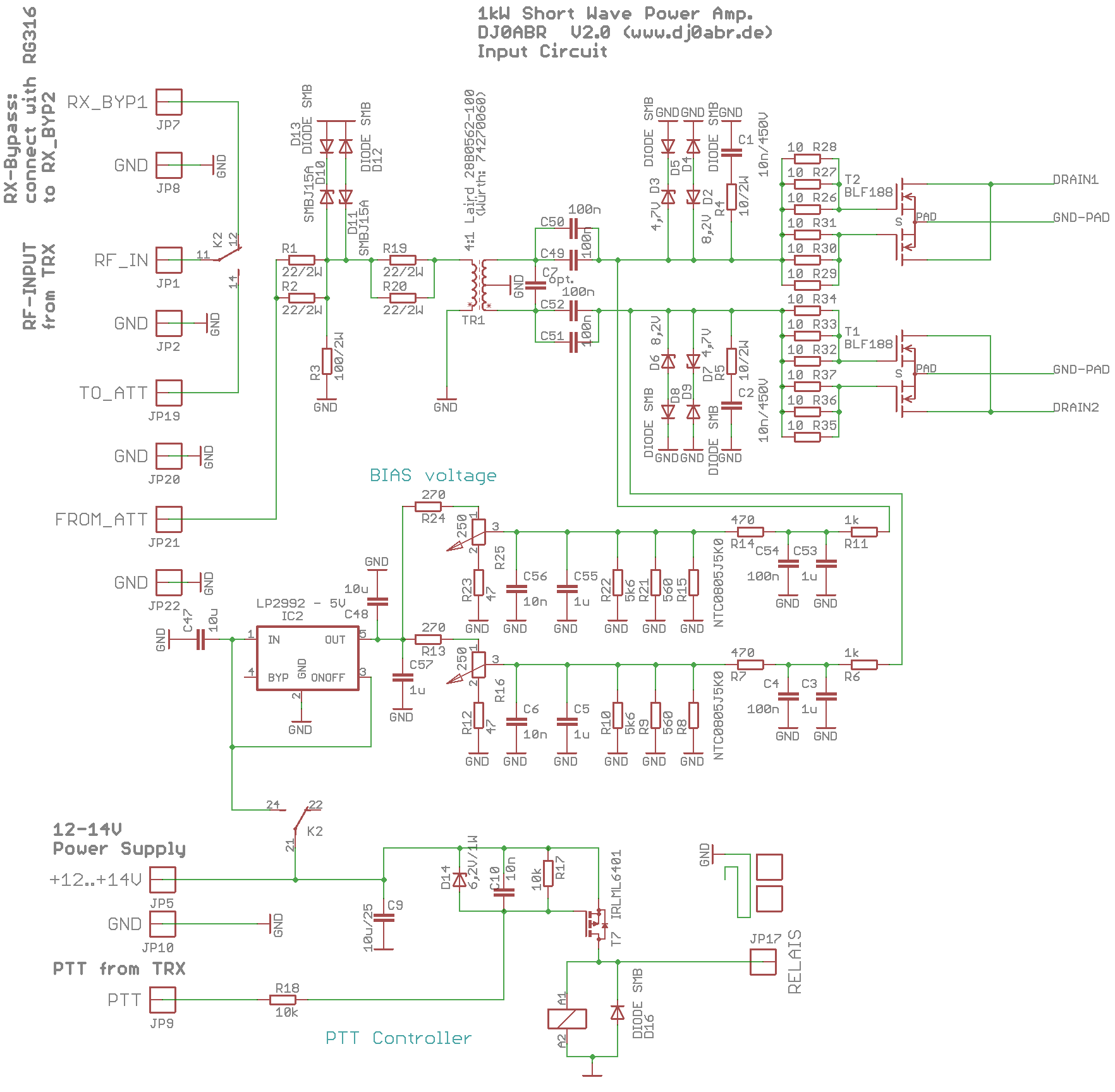
Input circuit (click to zoom):
The power from a transceiver is conencted to RF_IN. After passing the RX/TX Relais it goes to TO_ATT whee an external input attenuator can be connected. I highly recommend to use a -10dB attenuator which can easily be build with RF-Film power resistors (2x100 ohms, 2x33ohms). The signal goes from the attenuator to FROM_ATT).
Then the signal goes through an additional on-board attenuator which uses a special diode to clip high input voltages. This is the first stage of the input protection.
A 4:1 transformer matches the 50 ohms input to the gate load and generates the symmetrical signals for the LDMOS transistor. The second gate protection is made with two zener diodes. I have already "tested" this protection by driving the amp with 100W input, by mistake. The amp was not damaged, just the resistors of the input attenuator got very hot. So the protection is working well.
Important ! This circuit uses to separate trimmers for the BIAS voltage adjustment of the LDMOS. Now wen can adjust the two halfs of the AB amplifier separately. This concept showed an important advantage: By adjusting the BIAS and measuring the outpit with a spectrum analyser we can totally cancel out the first harmoic. This simplifies the design of the low pass filter a lot and allows to design filters with a very low pass band attenuation.
Output circuit (click to zoom):

TR2 and TR3 are "one" transformer. Even if physically build on thwo cores, logically this is only one transmission-line-transformer with an impedance ration of 1:9. This ratio is not the result of the number of windings, it is only the result of the circuit, any number of windings will give the same 1:9 ratio.
TR4 is the Balun to convert the symmetrical to an unsymmetrical signal. .
PCB:
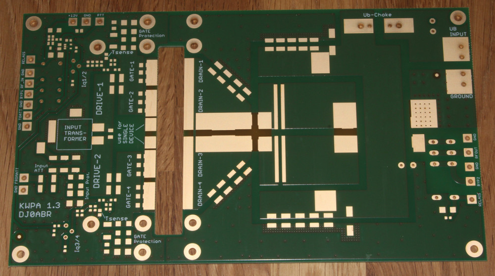
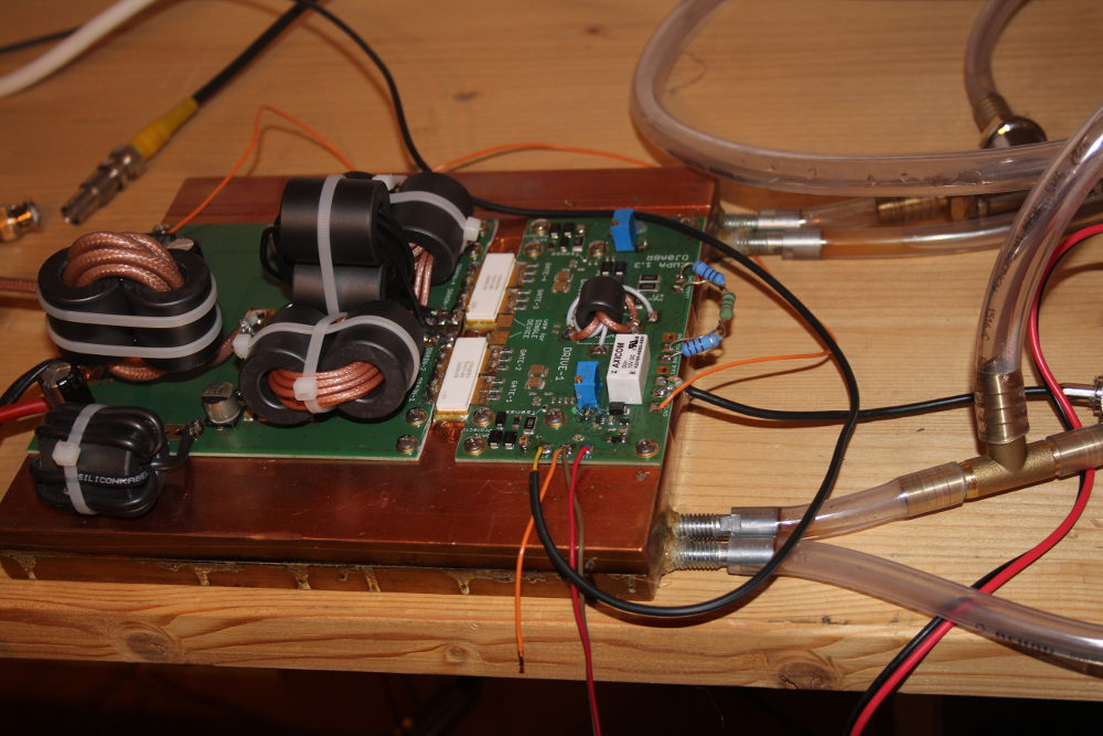
Input and Output circuits are on one single board which makes assembly more comfortable. After assembly of the SMD parts the board is cut into two halfs. The board has 70um copper and is gold plated.
This is the fully assembled board mounted on a heat spreader with water cooling channels. This video shows manufacturing of this cooler Youtube Video