The first prototype
This is the prototype. Only use these data if you have a prototype board. For the final layout see HERE.
Objective:
* about 3 to 6 watts output power
* about 15 to 18 dB gain
* Cascadable if higher gains are required
* very reasonably priced, material costs under 50.- if possible under 30.- Eur
* DIY should also be possible without measuring equipment
Finding a suitable concept:
Based on the desired performance data, the search for a suitable transistor began.
The choice fell on the MHT1008N (Freescale Semiconductor), which has indicated in the data sheet a maximum power of 12.5W at 28 volts. With luck you can expect half of this performance, but that would fit.
The adaptation of the transistor input and output to 50 ohms is usually done with strip lines, which are copper tracks in the layout. By appropriate choice of the impedance and length of the stripline, the desired transformations can be produced.
Fortunately, we did not have to start from scratch (which probably would not have worked), but Freescale has a reference layout with the correct adjustments. However, this layout requires Rogers 4350 board material, which is very expensive (for small quantities). However, with a maximum power of 10 watts, a PA can also work with normal FR4 board material. To keep the losses as low as possible we would choose the thinnest board material offered by our PCB manufacturer: 0,6mm thickness.
The next task was to convert the strip lines of the reference layout from Rogers to FR4 board material. DC1RJJ has agreed to do that because he has the required knowledge and the software. Based on his calculations, I modified the reference layout and had a test board created and manufactured.
the test board, which serves to check our calculations and the new layout:
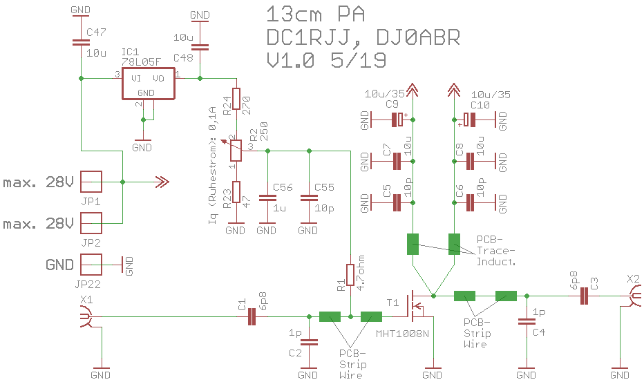
Circuit diagram of the test board:
the stripline and some capacitors of the reference layout have been changed, and bias current bias has been added.
Layout of the test board:
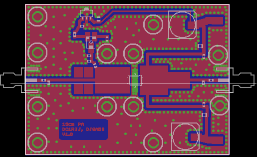
Board size: 77 x 56 mm
Bottom (blue): complete copper surface, no traces, no solder resist.
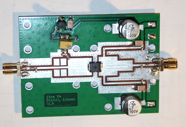
Finished prototype:
commissioning:
First, the DC voltage paths were tested and the quiescent current set to 100 mA as recommended in the data sheet.
The further tests were carried out with a supply voltage of 12V and also 24V.
The board was screwed onto a suitable heat sink. It has many 3mm holes which are all used for screws so that the boards have a very good contact with the heat sink. The transistor must transfer its heat trough vias in the board to the heat sink. That's not ideal, but common for this transistor package. Therefore I provided a particularly large number of plated-through holes below the transistor.
Adaptation and measurements:
the input matching was done by DC1RJJ. In the reference layout, there are four copper areas at the gate of the transistor, which can be connected as needed.
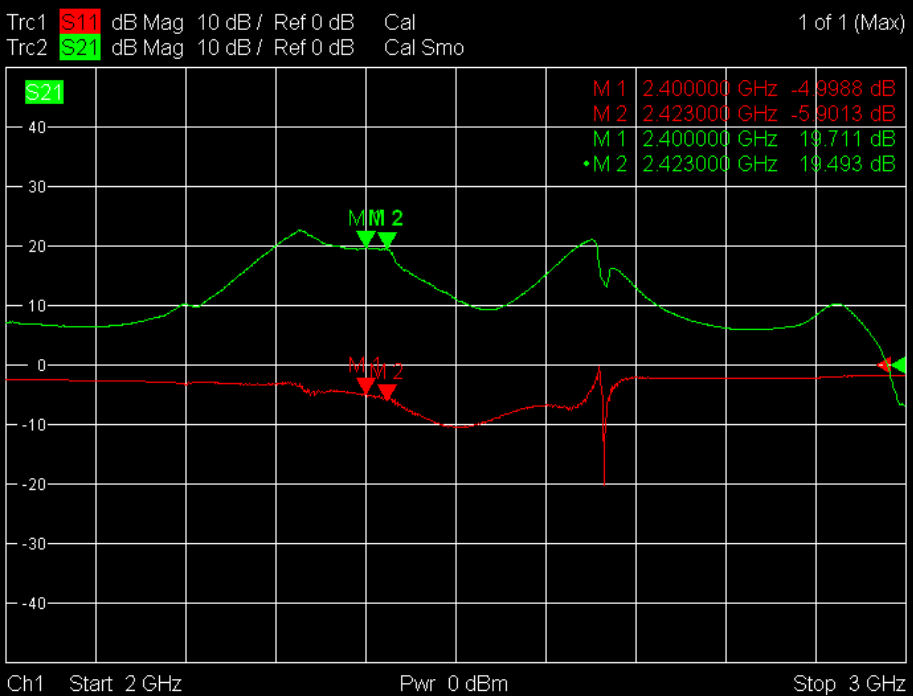
At first, the readings looked like this:
S11 (red) is the adaptation of the input, it was only -5dB, which corresponds to an input SWR of about 3.5: 1. Green is S21, the gain. It is actually lower than indicated (about 4dB) due to calibration problems with the analyzer.
Now the copper surfaces were connected in different configurations until the adjustment was right.
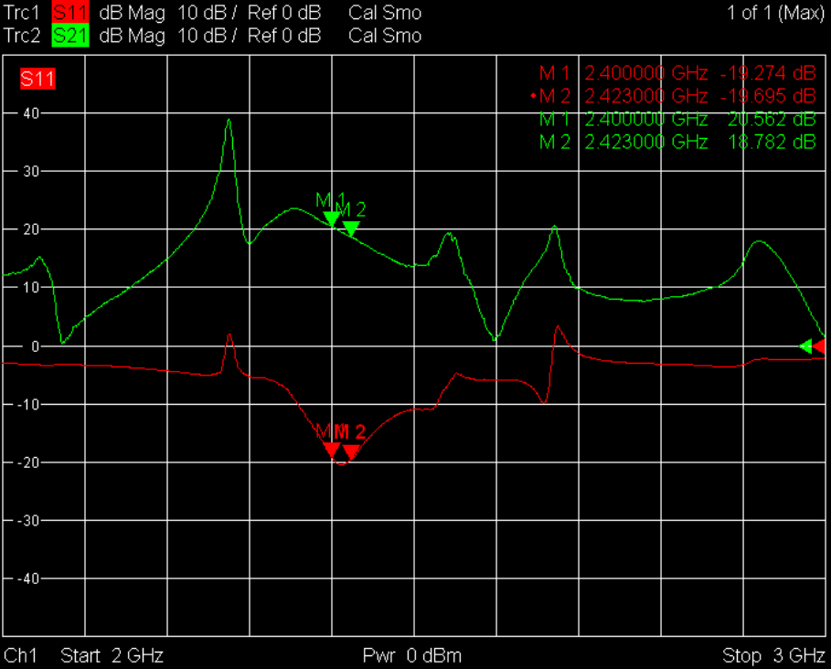
After matching, it looked like this:
at 12V supply voltage:
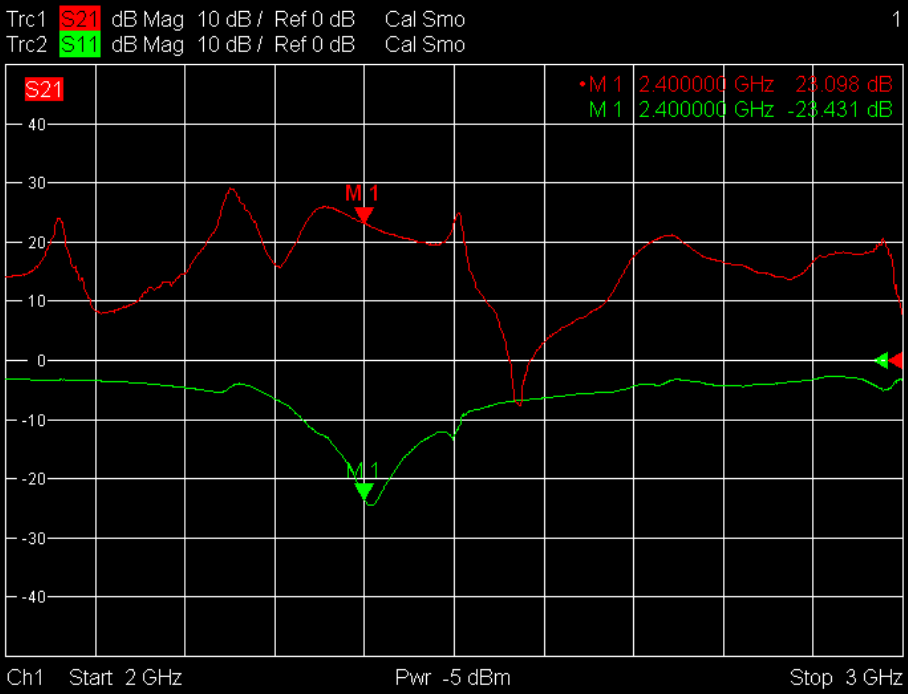
and with 24V supply voltage (red and green reversed):
S11, the input match is now better than -20dB, so the input SWR is better than 1.2: 1, a very useful value. The gain is approximately 17 to 18 dB at 12 volts (as before, the values displayed in the analyzer are too high).
Measurement of the output power:
The following table shows the measured values at 5W and maximum output power:
| Ub | Output Power | Current | Drive Power | Gain |
| [V] | [W] | [A] | [mW] | [dB] |
| 12 | 5 | 0,85 | 100 | 17 |
| 24 | 5 | 0,48 | 63 | 19 |
| 12 | 7,9 | 1,1 | 400 | 13 |
| 24 | 10 | 0,68 | 200 | 17 |
These performance figures are peak values. The Mosfet is already in compression.
For a clean SSB signal about 30 to 40% of this maximum power can be used. This makes it clear that the PA must be operated with 24 volts (up to 28V). At an input power of 100mW (20dBm), a clean output power of about 3.5W (35dBm) can be expected.
You can also use 200mW input, then it generates 6.5 watts. That is the maximum. With an input power over 400 mW the transistor will be damaged !!!
You have to be careful not to over drive the PA's input.